PVD Research Systems

PVD 科研设备

Ultra-high vacuum magnetron sputtering platforms for metals, dielectrics and compound thin-film research.

超高真空磁控溅射平台,面向金属、介质与化合物薄膜研究。

Overview产品概述

Precision deposition for advanced thin-film research

面向先进薄膜研究的高精度沉积

Magnetron sputtering is a cutting-edge physical vapor deposition (PVD) technique widely used in glass manufacturing, electronics and solar energy. It enables thin films with exceptional precision, uniformity and durability — from energy-efficient building glass to functional automotive glass.

磁控溅射是一种尖端的物理气相沉积(PVD)技术,广泛应用于玻璃制造、电子与太阳能等行业,可沉积具有出色精度、均匀性与耐久性的薄膜——从节能建筑玻璃到功能性汽车玻璃。

SEMIVAC sputtering systems can be constructed with various chamber and source configurations for depositing metals and dielectric thin films. Standard research platforms are the JSD-300 (Ø300 mm chamber) and JSD-450 (Ø450 mm chamber) magnetron sputtering coaters, equipped with DC, RF and pulsed-DC power supplies to enable sequential or co-sputtering, with adjustable magnetron-to-substrate distance and substrate heating up to 700 °C with RF bias.

SEMIVAC 溅射系统可根据不同腔体与源配置构建,用于沉积金属与介质薄膜。标准科研平台为 JSD-300(Ø300 mm 腔体)与 JSD-450(Ø450 mm 腔体)磁控溅射镀膜机,配备 DC、RF 与脉冲 DC 电源,支持顺序溅射或共溅射;磁控源与基片间距可调,基片可加热至 700 °C 并施加 RF 偏压。

  • DC, RF & pulsed-DC power supplies for sequential or co-sputtering
  • 支持 DC、RF 与脉冲 DC 电源,可顺序溅射或共溅射
  • Adjustable magnetron-to-substrate distance for uniformity and deposition rate
  • 磁控源与基片间距可调,优化均匀性与沉积速率
  • Substrate heating up to 700 °C with RF bias
  • 基片可加热至 700 °C,支持 RF 偏压
  • Ultra-high vacuum design for clean, high-quality films
  • 超高真空设计,保证薄膜洁净与高品质
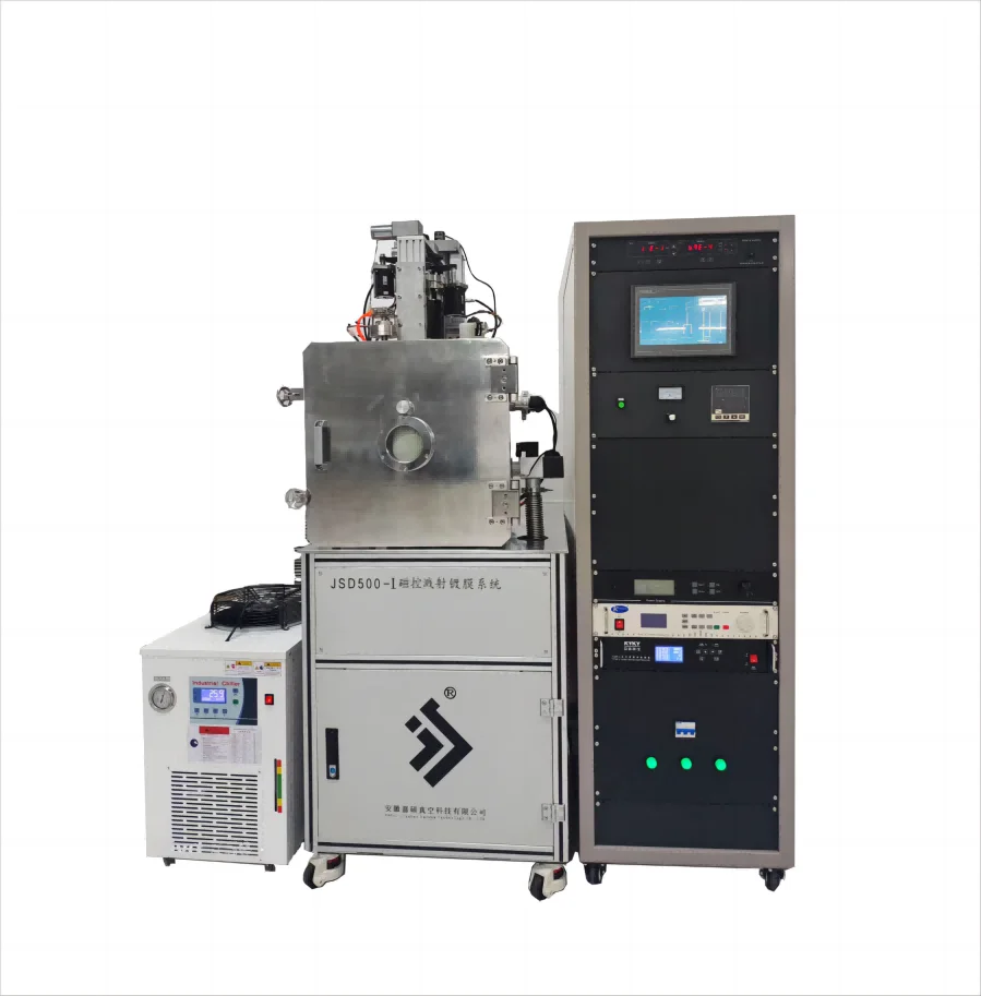
JSD-450 magnetron sputtering PVD research system
Corresponding Models对应产品型号

JSD series magnetron sputtering coaters for R&D

JSD 系列磁控溅射镀膜机,专为科研设计

The JSD series are single-chamber ultra-high vacuum magnetron sputtering systems built for research institutes and universities. Sputtering flux is directed at a rotating substrate holder for uniform films, and the systems can prepare elemental, compound, multilayer and co-sputtered thin films. The JSD-300 doubles as a specimen preparation tool for SEM and electron probe (EPMA) analysis under high-purity argon.

JSD 系列为单室超高真空磁控溅射系统,专为科研院所与高校设计。溅射束流朝向自转基片架,成膜均匀;可制备单质膜、复合膜、多层膜与共溅射薄膜。JSD-300 还可用于扫描电镜(SEM)与电子探针(EPMA)的试样制备,可在高纯氩气保护下进行多种离子处理。

JSD-300 magnetron sputtering coater

JSD-300 Magnetron Sputtering Coater

JSD-300 磁控溅射镀膜机

Compact single-chamber system with a Ø300 × H250 mm chamber and 1–2 JSD-R60 cylindrical targets — the economical choice for metals, dielectrics and multilayer research.

紧凑型单室系统,真空室 Ø300 × H250 mm,配备 1–2 支 JSD-R60 圆柱靶——金属、介质与多层膜研究的经济之选。

  • Base pressure ≤ 6.6×10⁻⁴ Pa
  • 极限真空度 ≤ 6.6×10⁻⁴ Pa
  • DC 0.5 kW & RF 0.5 kW (optional) power supplies
  • DC 0.5 kW 与 RF 0.5 kW(选配)电源
  • Substrate Ø60 mm, heatable to 700 °C, water-cooling option
  • 基片 Ø60 mm,可加热至 700 °C,可选水冷
  • Ideal for SEM / EPMA specimen preparation
  • 适用于 SEM / EPMA 试样制备
JSD-450 magnetron sputtering coater

JSD-450 Magnetron Sputtering Coater

JSD-450 磁控溅射镀膜机

Larger Ø450 × H350 mm single-chamber platform with three JSD-R60 cylindrical targets that run independently or simultaneously for co-sputtering of compound films.

大腔体 Ø450 × H350 mm 单室平台,配备三支 JSD-R60 圆柱靶,可独立或同时工作,支持化合物薄膜共溅射。

  • Base pressure ≤ 6.6×10⁻⁴ Pa
  • 极限真空度 ≤ 6.6×10⁻⁴ Pa
  • DC 500 W, RF 500 W & optional ion source power
  • DC 500 W、RF 500 W 与可选离子源电源
  • Substrate Ø100 mm, 30–120 rpm, heatable to 700 °C
  • 基片 Ø100 mm,30–120 转/分,可加热至 700 °C
  • Turbo pump 620 L/s (1200 L/s optional)
  • 分子泵 620 L/s(可选 1200 L/s)
Specification规格 JSD-300JSD-300 JSD-450JSD-450
Chamber真空室 Ø300 × H250 mm, single chamber, 304 SS, cylindrical vertical, flip-top lidØ300 × H250 mm,单室结构,304 不锈钢,圆筒形立式,上翻盖 Ø450 × H350 mm, single chamber, 304 SS, cylindrical vertical, top lid with liftØ450 × H350 mm,单室结构,304 不锈钢,圆筒形立式,顶盖带升降
Magnetron Sources磁控溅射源 1–2 × JSD-R60 cylindrical targets (Ø60 mm), independent or simultaneous1–2 支 JSD-R60 圆柱靶(Ø60 mm),可独立或同时工作 3 × JSD-R60 cylindrical targets (Ø60 mm), independent or simultaneous3 支 JSD-R60 圆柱靶(Ø60 mm),可独立或同时工作
Power Supplies电源 DC 0.5 kW, RF 0.5 kW (optional)DC 0.5 kW,RF 0.5 kW(选配) DC 500 W, RF 500 W, optional ion source powerDC 500 W,RF 500 W,可选离子源电源
Substrate基片 Ø60 mm, 1 pc, rotating holder, speed adjustableØ60 mm,1 块,自转基片架,转速可调 Ø100 mm, 1 pc, rotation 30–120 rpmØ100 mm,1 块,自转 30–120 转/分
Substrate Heating基片加热 Up to 700 °C, water-cooling option可加热至 700 °C,可选水冷 Up to 700 °C, water-cooling option, PID control (±2 °C)可加热至 700 °C,可选水冷,PID 控温(±2 °C)
Target–Substrate Distance靶基距 Adjustable可调 40–100 mm adjustable40–100 mm 可调
Ultimate Pressure极限真空度 ≤ 6.6×10⁻⁴ Pa≤ 6.6×10⁻⁴ Pa ≤ 6.6×10⁻⁴ Pa≤ 6.6×10⁻⁴ Pa
Pump-Down抽气时间 ≤ 8×10⁻⁴ Pa within 30 min30 分钟内 ≤ 8×10⁻⁴ Pa ≤ 8×10⁻⁴ Pa within 30 min30 分钟内 ≤ 8×10⁻⁴ Pa
Pumping System真空获得系统 Turbo pump (KYKY 620 L/s) + rotary vane pump分子泵(KYKY 620 L/s)+ 旋片机械泵 Turbo pump 620 L/s (1200 L/s optional) + rotary vane pump分子泵 620 L/s(可选 1200 L/s)+ 旋片机械泵
Typical Films典型薄膜 Metals, dielectrics, compounds, multilayers, SEM/EPMA specimens金属、介质、化合物、多层膜及 SEM/EPMA 试样 Metals, dielectrics, compounds, multilayers, co-sputtered films金属、介质、化合物、多层膜与共溅射薄膜

Non-standard chambers, target arrangements and process functions can be customized to match your research.

非标腔体、靶位布局与工艺功能均可按科研需求定制。

Applications典型应用

Where the technology is used

技术应用领域

Optical Coatings光学镀膜 ITO CoatingsITO 镀膜 Hard Coatings硬质涂层 Protective Coatings防护涂层 Microelectronics Patterning微电子图形化 TCO for OLEDOLED 用 TCO
Co-Sputtering共溅射 Multilayer Film Deposition多层膜沉积 Insulating Thin Films绝缘薄膜 Compound Film Fabrication化合物薄膜制备 Sequential Deposition顺序沉积 SEM / EPMA Specimen PrepSEM / EPMA 试样制备
Customization定制能力

Built around your process

围绕您的工艺定制

Chamber & Source Configurations

腔体与源配置

Various chamber sizes and multiple sputtering sources arranged for your specific thin-film stack.

多种腔体尺寸与多溅射源布局,满足您的特定膜系设计。

Process Control

工艺控制

Recipe-driven sequential and co-deposition control with accurate thickness management.

配方驱动的顺序沉积与共沉积控制,实现精确的膜厚管理。

R&D to Production

从研发到量产

Suitable for research institutions, universities and industrial manufacturers across various fields.

适用于科研机构、高校及各类工业企业。

Related Research Systems相关科研系统

Complementary deposition platforms

配套沉积平台

Beyond magnetron sputtering, SEMIVAC offers a full range of companion research systems for universities and institutes — electron beam evaporation, plasma-enhanced CVD, pulsed laser deposition and organic/metal evaporation.

除磁控溅射外,SEMIVAC 还提供面向高校与科研院所的全系列配套设备——电子束蒸发、等离子体增强 CVD、脉冲激光沉积与有机/金属蒸发系统。

Electron beam evaporation coater

E-Beam Evaporation Coater (400–500)

电子束镀膜机(400–500)

E-gun 8–10 kV / 6–8 kW plus resistance sources; substrate Ø400 mm heatable to 300 °C; quartz crystal thickness monitor.

E 型电子枪 8–10 kV / 6–8 kW,配电阻蒸发源;基片 Ø400 mm,可加热至 300 °C;配备石英晶振膜厚仪。

PECVD system

PECVD System (350-P)

PECVD 系统(350-P)

Chamber Ø350 × H350 mm; RF 500 W with auto matcher; rotating heated electrode RT–600 °C (±3 °C); MFC gas control; touchscreen + PLC.

沉积室 Ø350 × H350 mm;RF 500 W 自动匹配;旋转加热电极室温–600 °C(±3 °C);MFC 气体控制;触摸屏 + PLC。

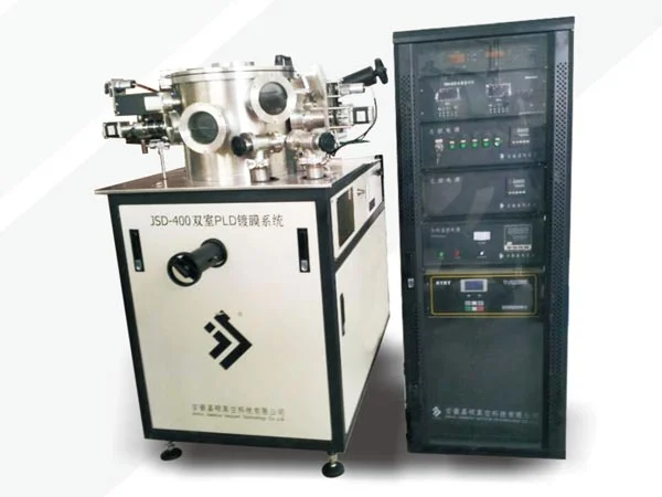
PLD system

PLD System (450)

脉冲激光沉积系统(450)

Base pressure ≤ 6×10⁻⁵ Pa; 4-station rotating targets with shields; substrate heating with PID ±1 °C; 2× MFC gas control.

极限真空 ≤ 6×10⁻⁵ Pa;4 工位旋转靶(带屏蔽罩);PID 基片加热 ±1 °C;2 路 MFC 气体控制。

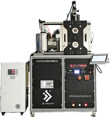
Organic and metal evaporation system

Organic / Metal Evaporation (JSD-400)

有机/金属蒸发系统(JSD-400)

Resistance evaporation for optical, low-melting-point metal and alloy films; multi-source configuration with optional substrate rotation, heating and negative bias.

电阻蒸发,面向光学薄膜、低熔点金属与合金膜;多源配置,可选基片旋转、加热与负偏压。

All systems are supplied with installation, commissioning, operator training and after-sales process support by SEMIVAC.

以上系统均由 SEMIVAC 提供安装、调试、操作培训与售后工艺支持。

Discuss your deposition process

讨论您的沉积工艺

Contact our engineers to define the right chamber, sources and power configuration.

联系我们的工程师,确定合适的腔体、源与电源配置。

Get in Touch 联系我们