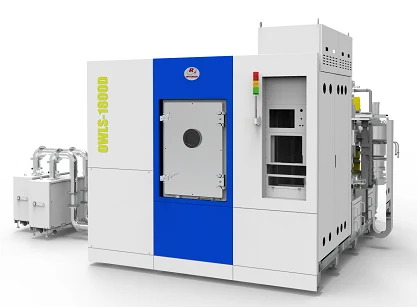
A Sputtering + Post-Oxidation/Nitridation with RPS (Remote Plasma Source) integrated system combines thin-film deposition and plasma oxidation/nitridation treatment in a single vacuum platform. The RPS module generates highly reactive oxygen radicals away from the substrate, enabling gentle and uniform oxidation/nitridation without direct plasma damage.
溅射 + 后氧化/氮化集成系统采用 RPS(远程等离子体源)技术,在同一真空平台内完成薄膜沉积与等离子体氧化/氮化处理。RPS 模块在远离基片的位置产生高活性氧自由基,实现温和、均匀的氧化/氮化,避免等离子体对基片的直接损伤。
The system integrates magnetron sputtering deposition and RPS post-oxidation/nitridation in one vacuum platform, covering the complete process chain from film deposition to surface oxidation/nitridation treatment.
系统将磁控溅射沉积与 RPS 后氧化/氮化集成于同一真空平台,覆盖从薄膜沉积到表面氧化/氮化处理的完整工艺链。

Load Lock → Sputtering Deposition → RPS Oxidation/Nitridation → Cooling → Unload
上料室 → 溅射沉积 → RPS 氧化/氮化 → 冷却 → 下料
Clean wafer loading without breaking vacuum.
在不破真空的情况下完成洁净上料。
Metal / film deposition via magnetron sputtering.
通过磁控溅射进行金属/薄膜沉积。
Remote plasma source generates oxygen radicals for controlled oxidation/nitridation.
远程等离子体源产生氧自由基,实现可控氧化/氮化。
Cooling before unloading protects film quality.
下料前冷却,保障薄膜质量。
Finished wafers are unloaded from the system.
成品晶圆从系统中取出。
Technology
DC magnetron sputtering
DC pulsed magnetron sputtering
RF magnetron sputtering
技术
直流磁控溅射
直流脉冲磁控溅射
射频磁控溅射
Materials
Al, Ti, Cr, Mo, W, Si
Cu, Ni, Ta
Metal alloys
Semiconductor materials
材料
Al、Ti、Cr、Mo、W、Si
Cu、Ni、Ta
金属合金
半导体材料
Functions
Dense thin-film deposition
Low-temperature processing
Excellent thickness uniformity
功能
致密薄膜沉积
低温工艺处理
优异的厚度均匀性
Remote Plasma Source Principle
O₂ / Ar gas → RPS plasma generation → Oxygen radicals (O) → Film oxidation/nitridation
远程等离子体源原理
O₂/Ar 气体 → RPS 等离子体生成 → 氧自由基(O)→ 薄膜氧化/氮化
Advantages
No direct ion bombardment
Low substrate damage
High oxidation/nitridation efficiency
Excellent uniformity over large substrates
优势
无直接离子轰击
基片损伤低
氧化/氮化效率高
大面积基片均匀性优异
Typical RPS Sources
RF Remote Plasma Source (13.56 MHz)
Microwave Remote Plasma Source (2.45 GHz)
ICP Remote Plasma Source
典型 RPS 源
射频远程等离子体源(13.56 MHz)
微波远程等离子体源(2.45 GHz)
ICP 远程等离子体源
| Feature | 特性 | Benefit | 收益 |
|---|---|---|---|
| In-situ process | 原位工艺 | No air exposure between deposition and oxidation/nitridation | 沉积与氧化/氮化之间不暴露大气 |
| RPS oxidation/nitridation | RPS 氧化/氮化 | Low damage, high-quality oxide formation | 低损伤、高质量氧化/氮化层 |
| Precise oxygen control | 精确氧量控制 | Better film stoichiometry | 薄膜化学计量比更优 |
| Single vacuum platform | 单一真空平台 | Higher productivity and lower contamination | 更高产能、更低污染 |
| Sequential process control | 顺序工艺控制 | Enables advanced multilayer structures | 支持先进多层结构制备 |
Metal oxide formation
High-k dielectric preparation
Gate stack engineering
Interface oxidation/nitridation treatment
金属氧化/氮化物制备
高介电常数介质层制备
栅极堆叠工程
界面氧化/氮化处理
Al → Al₂O₃ oxidation/nitridation
Ti → TiO₂ formation
Si → SiO₂ formation
Cr → Cr₂O₃ protective coatings
Al → Al₂O₃ 氧化/氮化
Ti → TiO₂ 制备
Si → SiO₂ 制备
Cr → Cr₂O₃ 保护涂层
Metal deposition followed by oxide conversion
Oxide-enhanced wear and corrosion resistance
金属沉积后氧化/氮化物转化
氧化/氮化物增强耐磨与耐腐蚀性能
Oxide semiconductor layers
Gas sensing films
Catalytic surfaces
氧化/氮化物半导体层
气体传感薄膜
催化表面
Fast wafer loading and unloading without breaking vacuum.
快速上下料,不破坏真空。
Clean wafer transfer between process chambers.
工艺腔室间洁净晶圆传输。
Thin-film deposition with magnetron sources.
采用磁控源进行薄膜沉积。
Remote plasma oxidation/nitridation treatment.
远程等离子体氧化/氮化处理。
Temperature control for process requirements.
按工艺要求控制温度。
Optional RF bias for film property tuning.
可选射频偏压,调控薄膜性能。
Quartz crystal microbalance thickness monitoring.
石英晶体微天平膜厚监控。
Optical emission spectroscopy for process control.
发射光谱法监控工艺过程。
Recipe-driven automation for repeatable processes.
配方驱动自动化,保证工艺可重复性。
This configuration creates a flexible in-situ PVD + plasma surface engineering platform suitable for semiconductor, optical coating, MEMS, and advanced materials research.
该配置构建了灵活的原位 PVD + 等离子体表面工程平台,适用于半导体、光学镀膜、MEMS 及先进材料研究。
Contact us for detailed configuration and process validation options.
联系我们获取详细配置与工艺验证方案。