Multidisciplinary engineering that turns research requirements into reliable vacuum solutions.
多学科工程能力,将研发需求转化为可靠的真空解决方案。
Backed by a team of experienced engineers and technical professionals in research, product design and manufacturing, Semivac International maintains long-term technical collaborations with leading universities — including the National University of Singapore, Singapore A*STAR and Temasek Polytechnic — and serves many industrial customers.
依托一支在研发、产品设计与制造领域经验丰富的工程师与技术团队,Semivac International 与新加坡国立大学、新加坡 A*STAR、淡马锡理工学院等顶尖高校保持长期技术合作,并服务众多工业企业客户。
Through continuous innovation and industry-academia cooperation, the company has accumulated extensive expertise in the design and manufacture of advanced vacuum equipment.
通过持续创新与产学研合作,公司在先进真空设备的设计与制造方面积累了丰富经验。
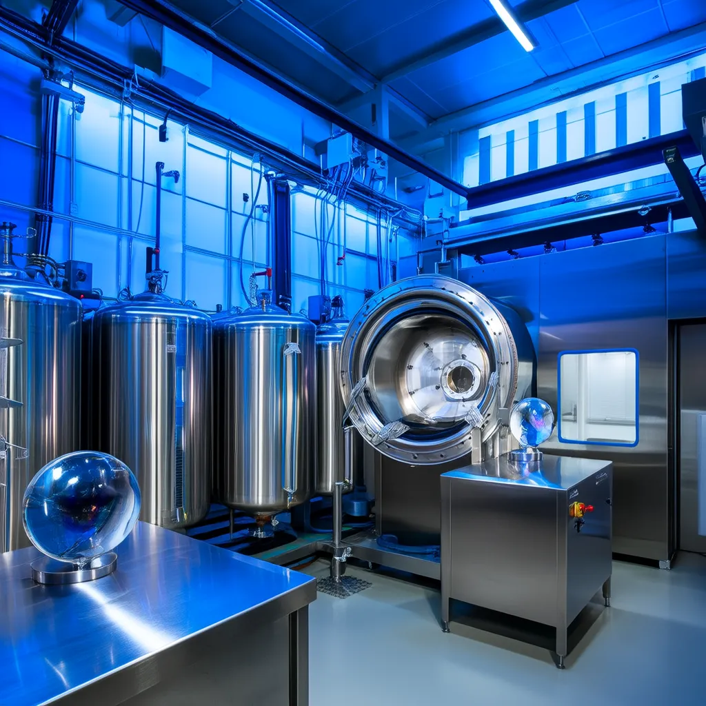
Ultra-high vacuum chambers, pumping systems and leak-tight design for clean thin-film deposition.
超高真空腔室、抽气系统与密封设计,保障洁净薄膜沉积。
DLC, oxide and compound films with engineered microstructure and properties.
DLC、氧化物与化合物薄膜,微观结构与性能可工程化调控。
Wafer handling, robotic transfer and recipe-driven process automation.
晶圆传输、机械手搬运与配方驱动的工艺自动化。
RF, DC, pulsed-DC and microwave power for stable plasma and sputtering processes.
RF、DC、脉冲 DC 与微波电源,保障等离子体与溅射工艺稳定。
Chambers, cathode assemblies, drums and fixtures engineered for uniformity and reliability.
腔体、阴极组件、转鼓与夹具设计,兼顾均匀性与可靠性。
Process control, optical thickness monitoring and testing & inspection equipment.
工艺控制、光学膜厚监控与检测检验设备。
We help you choose and combine the right deposition processes for your materials and device targets.
我们协助您为材料与器件目标选择并组合合适的沉积工艺。
Our engineers can help define the process path and system configuration for your application.
我们的工程师可协助定义适合您应用的工艺路线与系统配置。