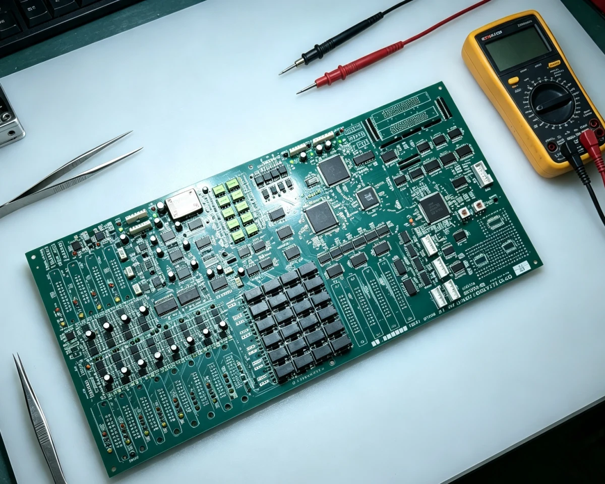
From reverse engineering to complete product development — board copying, chip decryption, design & re-layout, rapid manufacturing, SMT assembly and prototype making under one roof.
从逆向解析到完整产品开发——抄板、芯片解密、设计改板、快速制造、SMT 贴装与样机制作,一站式完成。
PCB reverse engineering is the process of analyzing a finished printed circuit board to recreate the original design files — schematic, layout, BOM and Gerber files — without access to the manufacturer's documentation.
PCB 逆向工程是对成品电路板进行分析,以重建原始设计文件——原理图、布局、BOM 与 Gerber 文件,全程无需制造商文档。
In simple terms, you are working backwards. Forward engineering goes schematic → layout → fabrication. Reverse engineering goes fabrication → layout → schematic. The end result is a complete design package that lets you repair, replicate or improve the board.
简单来说,就是"反着做"。正向工程是 原理图 → 布局 → 制造;逆向工程是 制造 → 布局 → 原理图。最终成果是完整的设计资料包,可用于维修、复制或改进电路板。

With professional PCB reverse engineering techniques and advanced tools, we can copy single-layer, double-layer and multi-layer printed circuit boards, including high-difficulty boards with blind and buried vias — restoring full design data for repair, replication or improvement.
依托专业的 PCB 抄板技术与先进的抄板工具,可抄制单层、双层、多层 PCB 电路板,并能对盲埋孔等高难度 PCB 电路板完成抄板工作,为维修、复制或改进恢复完整设计数据。
Building on our reverse engineering expertise, we cover the whole board development chain: recover locked chips, re-design or modify the layout, manufacture multi-layer boards in small batches, assemble them with SMT and validate with prototypes — all coordinated by one team.
依托逆向工程经验,我们覆盖电路板开发全链条:解锁受保护芯片、重新设计或改板、小批量制造多层板、SMT 贴装并完成样机验证——由同一团队一站式协调完成。
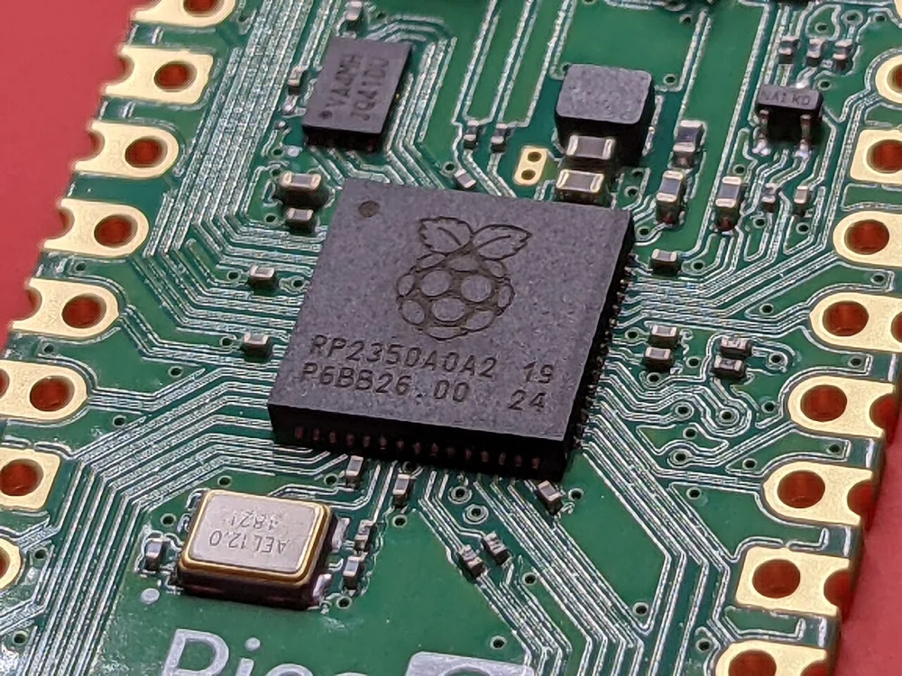
Deep research into MCU algorithms, architectures and processes to recover locked single-chip devices.
深入研究单片机算法、架构与工艺,解锁受保护的单片机设备。
Small-batch, multi-lot production for high-, mid- and low-end and special products.
小批量多批次生产体系,满足高中低端及特殊产品需求。
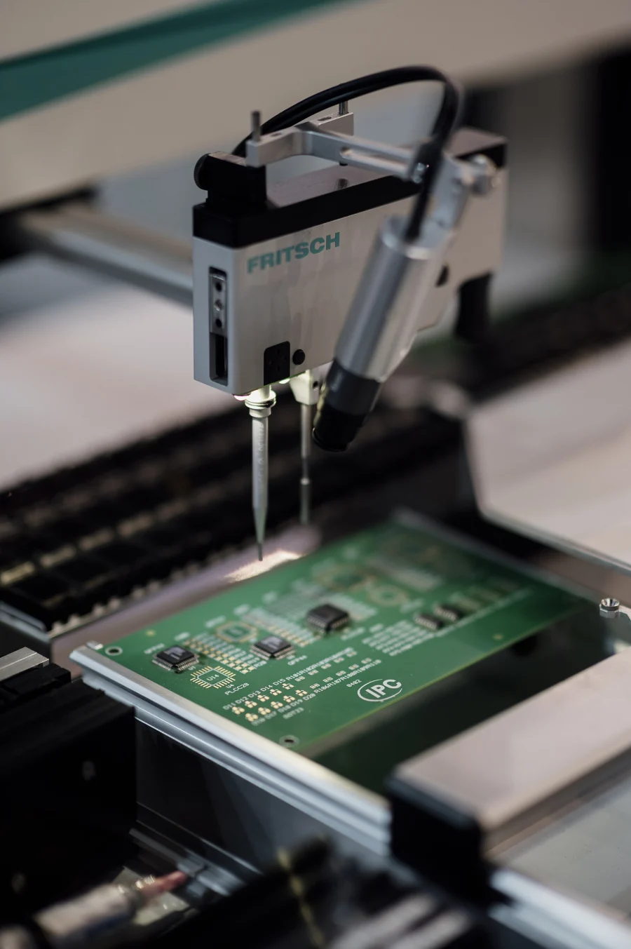
Placement, through-hole, post-soldering, testing and assembly with 10+ years of OEM/ODM experience.
贴片、插件、后焊、测试与组装,十余年 OEM/ODM 加工经验。
Multiple design proposals from your expectations, then build and iterate the prototype.
从客户期望出发提供多套设计方案,完成样机制作与迭代。
High-speed, high-density and mixed-signal design — flex, rigid-flex, HDI and blind/buried via.
高速高密数模混合设计,支持柔性板、刚柔结合板、HDI、盲埋孔。
The work combines four disciplines, each contributing to a complete, accurate design package.
工作融合四个环节,共同构成完整、准确的设计资料包。
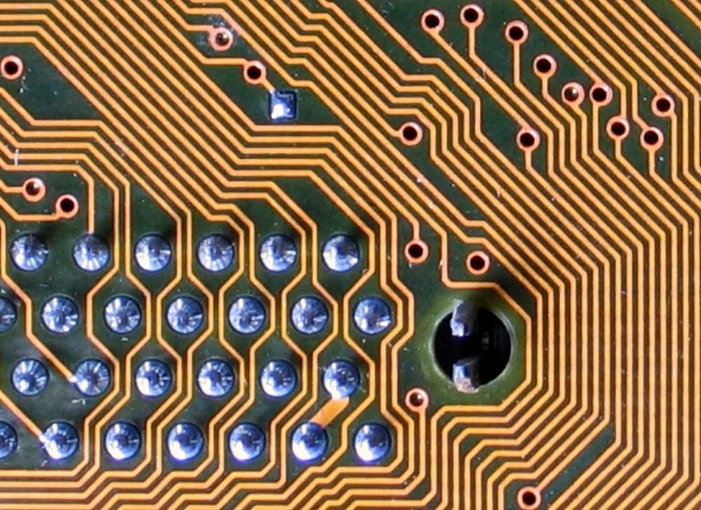
High-resolution imaging of every layer captures traces, vias, pads and component placement in detail.
对每一层进行高分辨率成像,完整记录走线、过孔、焊盘与元件布局。
Continuity checks and signal mapping reconstruct the electrical connectivity and netlist of the board.
通过导通性检查与信号映射,重建电路板的电气连接关系与网络表。
Part numbers and values are extracted from every component for an accurate BOM.
提取每个元器件的型号与参数,生成准确的 BOM 物料清单。
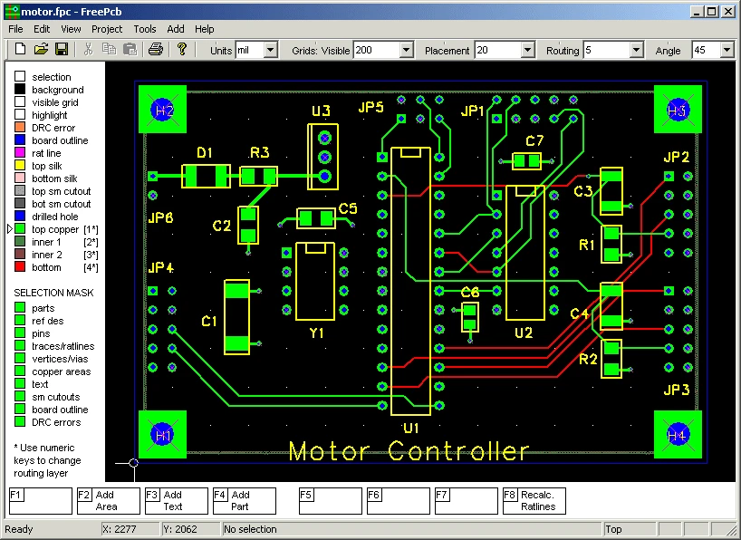
The schematic is rebuilt in EDA software, ready for review, modification and manufacturing.
在 EDA 软件中重建原理图,可直接用于审阅、修改与制造。
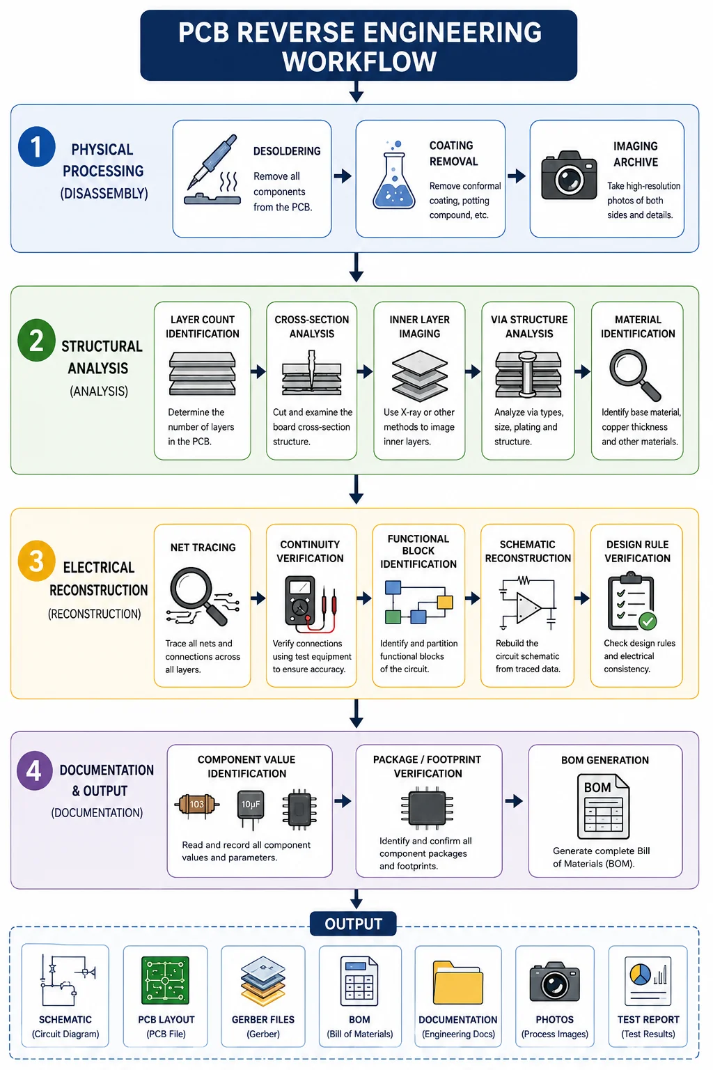
PCB reverse engineering disassembles and analyzes the physical board to restore the full design package — schematic, PCB layout and BOM — widely used for replication, fault analysis and documentation completion.
PCB 逆向工程通过对已有实物电路板拆解分析,还原出原理图、PCB 版图、BOM 物料清单等全套设计资料,多用于仿制、故障分析与文档补全。
Prepare the bare board for analysis
将成品板还原为可分析的裸板
Every component is removed from the PCB safely, preserving parts for later identification.
安全拆除 PCB 上全部元器件,保留器件供后续识别。
Conformal coatings, potting compounds and other protective layers are cleared for clear inspection.
清除三防漆、灌封胶等保护层,露出清晰可检的板面。
High-resolution photos of both sides and key details are archived as the project baseline.
对电路板正反面及关键细节拍摄高清照片并归档,作为项目基线。
Understand how the board is built, layer by layer
逐层还原电路板的制造结构
The total number of copper layers in the stack-up is determined.
确定 PCB 叠层总数。
Physical cross-sectioning reveals the board’s internal layer structure.
通过切片观测电路板截面内部结构。
X-ray and other imaging techniques capture the inner-layer routing.
使用 X 射线等手段获取内层走线图像。
Via type, dimensions and plating structure are analyzed in detail.
解析过孔类型、尺寸与镀层结构。
Substrate material, copper foil thickness and other board parameters are confirmed.
确认基材、铜箔厚度等板材参数。
Rebuild the connectivity of every net
重建每一根网络的电气连接
Nets and connections are traced across every layer of the board.
追踪所有层的网络与连接关系。
Instruments verify each connection to guarantee electrical accuracy.
用仪器测试核对连接,确保电气准确。
Circuits are divided and mapped into recognizable functional units.
划分并识别各电路功能单元。
The schematic is rebuilt from the traced data, block by block.
基于追踪数据逐步还原电路原理图。
Design rules and electrical consistency are validated before delivery.
校验设计规则与电气一致性,确保交付质量。
Deliver a complete, manufacturable design package
输出可直接投产的完整设计资料
All component values and markings are read and recorded.
读取并记录全部器件参数与丝印。
Packages and footprints are verified against the actual pads.
核对元器件封装与焊盘一一对应。
A complete, procurement-ready BOM is delivered with the files.
输出完整 BOM 物料清单,可直接用于采购。
Rebuilt in EDA software, ready for review and re-engineering.
在 EDA 软件中重建,可直接审阅与再设计。
Layer stack, traces, vias and pad geometry reproduced accurately.
精确还原层叠结构、走线、过孔与焊盘几何。
Component list with part numbers and values for procurement.
含型号与参数的元器件清单,便于采购。
Manufacturing-ready files for fabrication and assembly.
可直接用于制造与贴装的加工文件。
Legacy boards without documentation are reproduced from the rebuilt design files.
无文档的旧板卡,依据重建的设计文件进行复制生产。
Failures are traced down to netlist level for precise diagnosis and targeted repair.
对故障进行网络级定位诊断,实现精准维修。
Missing schematics, layouts and BOMs are restored for legacy equipment.
为老旧设备补全缺失的原理图、版图与物料清单。
Tell us about the board, its layers and your goal — repair, replication or improvement.
告诉我们电路板情况、层数与目标——维修、复制还是改进。