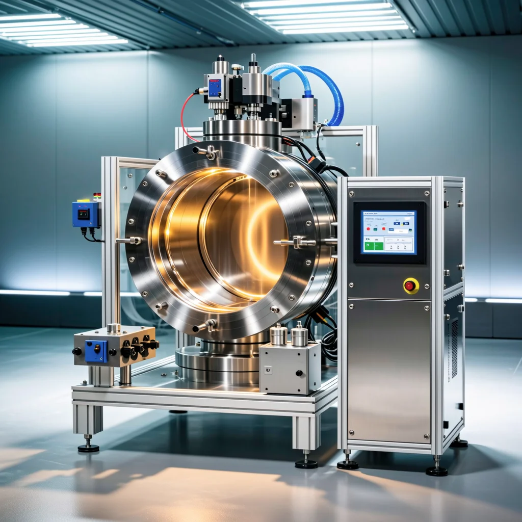
Magnetron sputtering is a cutting-edge physical vapor deposition (PVD) technique widely used in industries such as glass manufacturing, electronics and solar energy. This technology enables the deposition of thin films with exceptional precision, uniformity and durability. From enhancing energy efficiency in buildings to improving the functionality of automotive glass, magnetron sputtering plays a pivotal role in modern manufacturing.
How it works
In magnetron sputtering, a plasma is confined near the target surface by a magnetic field. Ions from the plasma bombard the target, ejecting atoms that travel to the substrate and condense into a thin film. The magnetic confinement keeps electrons near the target, enabling efficient ionization at lower pressures and voltages.
Flexible process configuration
SEMIVAC sputtering systems can be constructed with various chamber and source configurations for depositing metals and dielectric thin films onto substrates. Key configuration options include:
- Power supplies: DC, RF and pulsed-DC to enable sequential or co-sputtering
- Geometry: adjustable magnetron-to-substrate distance to achieve desired uniformity and deposition rate
- Temperature & bias: substrate heating up to 800 °C with RF bias
Applications
The technology supports a wide range of applications, including:
- Optical coatings and ITO coatings
- Hard coatings and protective coatings
- Microelectronics patterning
- TCO in OLED applications
With ultra-high vacuum design and precise process control, magnetron sputtering remains one of the most versatile and reliable ways to produce advanced thin films — from the research lab to industrial production.
磁控溅射是一种尖端的物理气相沉积(PVD)技术,广泛应用于玻璃制造、电子与太阳能等行业。该技术可沉积具有出色精度、均匀性与耐久性的薄膜。从提升建筑能效到改善汽车玻璃功能,磁控溅射在现代制造业中发挥着关键作用。
工作原理
在磁控溅射中,磁场将等离子体约束在靶材表面附近。等离子体中的离子轰击靶材,溅射出的原子飞向基片并凝聚成薄膜。磁约束使电子保持在靶材附近,从而在较低气压与电压下实现高效电离。
灵活的工艺配置
SEMIVAC 溅射系统可根据不同腔体与源配置构建,用于在基片上沉积金属与介质薄膜。关键配置选项包括:
- 电源:DC、RF 与脉冲 DC,支持顺序溅射或共溅射
- 几何:磁控源与基片间距可调,实现所需的均匀性与沉积速率
- 温度与偏压:基片加热最高 800 °C,支持 RF 偏压
应用领域
该技术支持广泛的应用,包括:
- 光学镀膜与 ITO 镀膜
- 硬质涂层与防护涂层
- 微电子图形化
- OLED 应用中的 TCO
凭借超高真空设计与精确的工艺控制,磁控溅射依然是制备先进薄膜最通用、最可靠的方法之一——从研究实验室到工业生产。