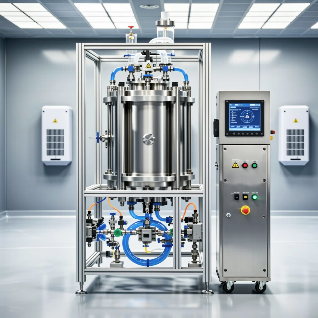
Atomic Layer Deposition (ALD) generally consists of a four-step cycle, which is repeated multiple times to reach the target deposition thickness. Unlike traditional CVD, ALD has a surface self-limiting characteristic, which is why it stands out among thin-film preparation techniques.
The four-step ALD cycle
Take the ALD of Al₂O₃ as an example, using precursors such as TMA (Al(CH₃)₃) and O₂:
- Step 1: Introduce TMA precursor vapor onto the substrate. TMA adsorbs on the substrate surface and reacts with it. By selecting appropriate precursors and process parameters, this reaction is self-limiting.
- Step 2: Purge all residual precursors and reaction byproducts.
- Step 3: Irradiate the surface with low-damage remote plasma containing reactive oxygen radicals to oxidize the surface and remove surface ligands. This reaction is also self-limiting due to the limited quantity of surface ligands.
- Step 4: Purge reaction byproducts from the chamber.
Only Step 3 differs between thermal and plasma-based processes: thermal processes utilize H₂O, while plasma processes employ O₂ plasma. Since each ALD cycle deposits a sub-angstrom to angstrom-scale thin film, the deposition process can be controlled at the atomic level.
Key advantages of ALD
- Precise film thickness control by adjusting the number of reaction cycles — atomic-level thickness
- Friendly deposition temperature, RT – 400 °C
- Excellent conformality on various substrate shapes, including high-aspect-ratio and complex 3D structures
- Large-area uniformity, thanks to saturated chemisorption of precursors
- No need to control precursor/reactant flow uniformity, due to self-limiting behavior
- Smooth, dense, pinhole-free films
- Suitable for interface modification and multi-component nanolaminate structures
- Scalable to production
Thermal ALD vs. Plasma-Enhanced ALD
Thermal ALD achieves highly conformal coatings even on high-aspect-ratio and complex structures, and is applicable to a wide variety of materials. Plasma-enhanced ALD (PE-ALD) expands the available precursor chemistry portfolio and yields superior film quality:
- Plasma enables low-temperature processes, while remote plasma sources maintain minimal plasma-induced damage
- Water is no longer required as a co-reactant, shortening purge duration between cycles
- Improved impurity elimination — lower resistivity and higher film density
- Efficient metal deposition via hydrogen plasma treatment
- Precise control over stoichiometry, phases and phase transformations
- Mitigated nucleation delay; in-situ chamber plasma cleaning available
Available material families
ALD supports dozens of oxides, nitrides, metals, fluorides, sulfides and organic hybrid materials — including Al₂O₃, HfO₂, SiO₂, TiO₂, ZnO, TiN, TaN, Si₃N₄, Pt, Ru, Pd, W, MgF₂, ZnS and more.
原子层沉积(ALD)通常由四步循环组成,根据目标沉积厚度重复多次。与传统 CVD 不同,ALD 具有表面自限制特性,这也是它在众多薄膜制备技术中脱颖而出的原因。
ALD 四步循环
以 Al₂O₃ 的 ALD 为例,使用 TMA(Al(CH₃)₃)和 O₂ 等前驱体:
- 第一步:将 TMA 前驱体蒸汽引入基片表面。TMA 在基片表面吸附并发生反应。通过选择合适的前驱体与工艺参数,该反应具有自限制性。
- 第二步:吹扫所有残留前驱体与反应副产物。
- 第三步:用含活性氧自由基的低损伤远程等离子体辐照表面,氧化表面并去除表面配体。由于表面配体数量有限,该反应同样具有自限制性。
- 第四步:从腔室中吹扫反应副产物。
热工艺与等离子体工艺仅在第三步有所不同:热工艺使用 H₂O,等离子体工艺使用 O₂ 等离子体。由于每个 ALD 循环沉积亚埃至埃级薄膜,沉积过程可实现原子级控制。
ALD 的主要特点
- 通过调节反应循环次数精确控制薄膜厚度——原子级厚度
- 沉积温度友好,室温 – 400 °C
- 适用于各种形状的衬底,在高深宽比结构与复杂三维结构中保形性优异
- 前驱体饱和化学吸附,保证大面积均匀性
- 基于自限制特性,无需控制前驱体或反应物流量均匀性
- 薄膜光滑、致密、无针孔
- 适合界面修饰与多组元纳米叠层结构
- 具备规模化生产能力
热 ALD 与等离子体增强 ALD
热 ALD 即使在高深宽比与复杂结构上也能获得高保形涂层,适用材料广泛。等离子体增强 ALD(PE-ALD)扩展了前驱体化学体系,可获得更优异的薄膜质量:
- 等离子体支持低温工艺,远程等离子体源保持极低的等离子体损伤
- 不再需要水作为共反应物,缩短循环间吹扫时间
- 杂质清除更彻底——电阻率更低、薄膜密度更高
- 通过氢等离子体处理实现高效的金属沉积反应
- 精确控制化学计量、物相与相变
- 缓解成核延迟;可选原位腔室等离子体清洗
可沉积材料体系
ALD 可沉积数十种氧化物、氮化物、金属、氟化物、硫化物与有机杂化材料——包括 Al₂O₃、HfO₂、SiO₂、TiO₂、ZnO、TiN、TaN、Si₃N₄、Pt、Ru、Pd、W、MgF₂、ZnS 等。